ПРОДУКТЫ:
|
MX-IR / BX-IR
These IR Imaging Systems contain dedicated IR objective lenses and components that are corrected for chromatic aberrations and designed for 700-1300nm wavelengths.


Описание:Non-destructive Internal Observation of Semiconductor DevicesWith the demand for thinner and more compact electronic components, it becomes increasingly important to perform internal inspection to ensure product intergrity. A near-infrared microscope supports non-destructive inspection and analysis of regions blocked to visible light, including SiP (System in Package), stacked package, and CSP (Chip Size Package). Non-destructive Failure Analysis of Flip Chip PackageIn the case of the flip chip bonding, the bonding sections and patterns are inaccessible after packaging for inspection using a routine optical microscope. With a near-infrared microscope, however, non-destructive internal observation of an IC chip after packaging is possible by the transmission properties of silicon. This technique makes failure analysis of the flip chip package a simple one and is also effective for identifying locations to be processed with FIB (Focused Ion Beam). Chip Damage Due to Environmental Testing on Wafer-level CSP'sNon-destructive inspection of wafer level CSP detects changes due to heat or moisture during testing. In addition, leaks due to fusion or corrosion of copper wiring and peeling of resin can be clearly observed. 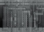
Aluminium Wiring (Back-side) 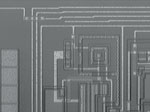
Solder Evaluation 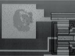
Electrode (Back-side) Compatible with the Olympus MX & BX Family of MicroscopesMX Series for Semiconductor InspectionThis series is capable of observing larger samples such as 150-300mm wafers. 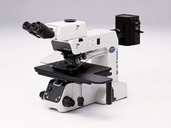
Semiconductor & Flat Panel Display Inspection Microscope 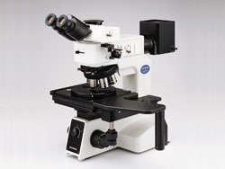
Industrial Inspection Microscope BX Series for Materials Inspection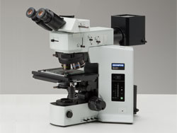
Motorized System Microscope for Reflected and Transmitted Light BXFM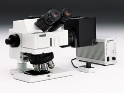
Compact microscope unit Its compact design allows for a easy integration into larger equipment.
* Please contact Olympus through Olympus Home Page for IR camera and imaging software.
|
- Продукты
- Передовые решения неразрушающего контроля
- Дефектоскопы
- Интегрированные системные решения в области НК
- Толщиномеры
- Компоненты микроскопов
- Оптические измерительные системы
- Видеоскопы, бороскопы
- Высокоскоростные видеокамеры
- Анализаторы XRF и XRD
- Микроскопия
- Semiconductor & Flat Panel Display Inspection
- Инвертированные металлургические микроскопы
- Лазерные конфокальные микроскопы
- Модульные микроскопы
- Объективы
- Опто-цифровые микроскопы
- Поляризационные микроскопы
- Программное обеспечение для анализа изображений
- Прямые металлургические микроскопы
- Стерео микроскопы
- Цифровые камеры
- ПРИМЕНЕНИЕ
- Технологии
- Новости
- события
- Тех.поддержка
- Контакты